In-situ observation of structural changes by the metal-to-semiconductor transition in lead telluride
Lead telluride is an important thermoelectric material but its metal-to-semiconductor transition above 230 °C is not fully understood. Here, atomic-resolution transmission electron microscopy provides structural insights into this transition, explaining the metallic behavior by local structural changes leading to the formation of a dislocation network within the rock salt structure.
Already in his first report 1822 about the discovery of thermoelectricity, he described Bleiglanz (galena), a natural form of lead sulfide, as a material yielding in combination with another substance the electrical current, if exposed to a temperature gradient. Using lead telluride-based materials in radioisotope thermoelectric generators, NASA successfully realized several space research programs. Potential applications of thermoelectrics such as waste heat recovery in the automotive industry or in power plants are in discussion. At least, thermoelectric generators found their way in every day’s life e.g. in smartwatches powered by body heat..
The electronic properties of lead telluride (PbTe) are still of high-ranking scientific interest and relevance for applications as far as thermal cycling stability of the material concerns due to the incomplete understanding of the metal-to-semiconductor transition at temperatures around 230 °C. As a reason for such behavior, the presence of excess atoms after the single-crystal growth and vaporization of tellurium from the specimens were discussed besides the creation and healing of defects due to mechanical milling and sintering, respectively. At least, excitation of electron-hole pairs with the formation of structural defects at elevated temperatures and temperature-dependent band crossing were also considered as reasons for the electronic transport behavior of PbTe. All these approaches assume that the crystal structure of PbTe remains basically unchanged.
In order to reveal the structural reasons for this specific electronic transition, a temperature-dependent in-situ atomic-resolution transmission electron microscopy study was performed on a single p-type crystal of lead telluride. Below the transition temperature at 230 °C, the formation of a dislocation network due to shifts of the NaCl-like atomic slabs perpendicular to {100} was observed. This local structure modification leads to the appearance of in-gap electronic states and causes metal-like electronic transport behavior. The dislocation network disappears with increasing temperature, yielding semiconductor-like electrical conductivity, and re-appears after cooling to room temperature restoring the metal-like behavior.
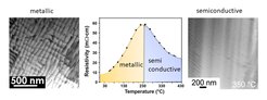
 Dislocation pattern of metallic PbTe at room temperature. (center) Temperature dependent resistivity measurements reveal metallic behavior below 230 °C, and semiconductive behavior over the transition temperature.")
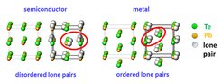
The shifts of atomic slabs perpendicular to {100} are caused by ordering of the stereochemically active lone pairs on lead atoms below the characteristic value of 230 °C. This causes changes in the electronic structure. The gap in the band structure of the ideal PbTe rock salt-type structure closes, and the material behaves like a metal in electronic transport measurements. Temperature increase above the characteristic value leads to a lone-pair disorder, and the crystal structure recovers the NaCl lattice and becomes semiconducting.
 Pristine atomic arrangement in NaCl-type PbTe and corresponding disordered lone-pairs scenario leading to lone-pair repulsive interaction marked with red circle. (right) Atomic arrangement with layers shifted by (0.25 0 0) reducing the repulsion between the lone-pairs.")