Spintronic goes chiral
Spintronic devices are based on using the fundamental spin of electrons to carry and store information. Their use would not require charge currents for their operation and would lead to improved energy efficiency with lower power consumption, higher data processing speed and better integration of memory and logic. However, suitable materials for new spintronic implementations are needed. Their fabrication as well as analysis require state-of-the-art methods from nanotechnology. This is why researchers of the Max Planck Institute for Chemical Physics of Solids and the Fraunhofer Institute for Photonic Microsystems IPMS have launched a joint project to investigate novel materials for spintronics. The project is being funded by Sächsische Aufbaubank.
Today, information processing and data storage technologies, for example for computer memories or hard disc drives in data centers, rely on the use of charge currents, which are innately associated with dissipation and high energy consumption. An alternative concept is offered by modern CMOS technology by using the magnetic moment carried by each electron, a quantum property called the ‘spin’. This will enable higher data processing speed and improved integration of memory and logic, with overall lower power consumption. To achieve these goals, one key requirement is to find new materials with the desired properties, which enable the generation of high efficiency of spin currents. This is where project “Topological Spintronics: CMOS-compatible materials from the B20 family” from the Max Planck Institute for Chemical Physics of Solids and the Fraunhofer Institute for Photonic Microsystems IPMS comes into play.
Chiral crystals are a promising class of materials that have remained largely unexplored for their potential use in spin-based electronics. In chiral materials, the atoms, of which the crystal is composed, can exist in two inequivalent arrangements, which look like the mirrored image of each another. This is similar to our right and left hands, which cannot be superimposed onto one another when the palms are both facing down - this is called chirality. The project aims to bridge the gap between understanding how chirality and spin currents are related and assessing the potential of chiral materials in electronic applications.
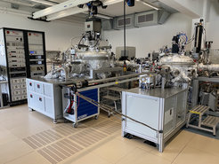
The Max Planck Institute for Chemical Physics of Solids and Fraunhofer IPMS have joined forces to explore the properties of nonmagnetic chiral materials and go beyond what is possible so far. The funding of Sächsische Aufbaubank for the project “Topological Spintronics: CMOS-compatible materials from the B20 family” enables the Dresden-based institutions to invest in new equipment for their state-of-the-art research and developments. The partners will use the excellent facilities for material growth to investigate new chiral materials with high charge-to-spin conversion. The materials will be further integrated into the production of high-quality magnetic stacks for future spintronic applications.

The group of Prof. Claudia Felser at the Max Planck Institute for Chemical Physics of Solids in Dresden is internationally known for their research on new topological quantum materials. “Spin and charge of electrons in chiral crystals open a new pathway for new high speed electronics, however it is a long way from a material to a device” says Prof. Claudia Felser, director at the Max Planck Institute in Dresden, “and with our colleagues from Fraunhofer IPMS, we will take a short cut to innovative technology”. “This project combined with our expertise in the field of topology, growth of high-quality epitaxial thin films and experience in spintronics will allow us to discover new spin Hall materials in the B20 family of compounds with high efficiency,” says Dr. Anastasios Markou, a group leader in Felser’s group.

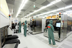
“This partnership will lift us up to the next level. With our colleagues from Max-Planck, we can work with materials that are not yet available in the CMOS world,” adds Dr. Maik Wagner-Reetz, who is responsible for the spintronics activities at IPMS. Fraunhofer IPMS’ Center Nanoelectronic Technologies develops solutions for processes and devices on 300 mm wafer level for the transfer of fundamental research results into industrial applications. The main core competences include the integration of new materials and 300 mm CMOS compatible device fabrication.


