In the framework of the ComCIGS-II project our team performs large scale ab-initio calculations on the materials related to thin film solar cells, focusing on three main areas of interest:
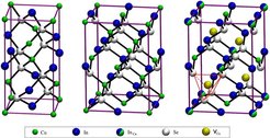
- the properties of the light absorber layer involving materials like CuInSe2, CuInS2, CuGaSe2, CuIn5Se8, (see Figure 1) and their interaction with various impurities from the buffer layer (CdS, Zn(O,S)), and the effect of Na and K dopants on the atomic and electronic structure of these materials

Figure 1: Conventional tetragonal unit cell of CuInSe2 (left). The tetragonal chalcopyrite-like CuIn5Se8 ordered vacancy compound (right) can be structurally understood as taking a √2 x √2 x 1 supercell of CuInSe2 (show in the center), and substituting two Cu atoms with In (denoted as InCu), and four Cu atoms are removed, leading to four pristine Cu-vacancy sites denoted as VCu.
- the chemisorption, diffusion and reaction of Se, Na, K and O on the Mo surfaces, adsorbate patterns, and simulating scanning tunnelling microscopy (STM) images to provide guidelines for future experiments (see Figure 2)
![Figure 2: The left panel shows the stability ranges for the most stable adsorption patterns/coverages of Se on the Mo(110) surface in equilibrium with a gas of Se2 molecules. The patterns corresponding to coverages θ=0.5 and θ=0.75 monolayers are sketched in their stability domain (the black box indicates the surface unit cell). On the right panel the simulated STM images are shown for the θ = 0.75 monolayer pattern for three different tip heights and a bias voltage V = −1 eV [1].](/2500535/standard_sans_both-1435237657.jpg?t=eyJ3aWR0aCI6MjQ2LCJvYmpfaWQiOjI1MDA1MzV9--5b9c24aef3717133da80c9dc3d3d66e2a1ede274)
Figure 2: The left panel shows the stability ranges for the most stable adsorption patterns/coverages of Se on the Mo(110) surface in equilibrium with a gas of Se2 molecules. The patterns corresponding to coverages θ=0.5 and θ=0.75 monolayers are sketched in their stability domain (the black box indicates the surface unit cell). On the right panel the simulated STM images are shown for the θ = 0.75 monolayer pattern for three different tip heights and a bias voltage V = −1 eV [1].
- the interaction between the Mo back-contact and the MoSe2 layer (see Figure 3) forming between the Mo surfaces and the light absorber layer, explicitly including the weak van der Waals forces into the calculations to describe the morphology of the Mo-MoSe2 interface, and to calculate its electronic properties

Figure 3: Crystal structure of bulk hexagonal MoSe2 (a), where a trigonal prism is highlighted with black color as a structural unit with one Mo atom in the trigonal prismatic hole of six Se atoms. The (10-10) and (11-20) surfaces of MoSe2 are shown in subfigures (b) and (c), respectively, where the slabs representing the surfaces are repeated periodically along the x and y directions, and the surfaces are perpendicular to the z axis.

![Figure 2: The left panel shows the stability ranges for the most stable adsorption patterns/coverages of Se on the Mo(110) surface in equilibrium with a gas of Se2 molecules. The patterns corresponding to coverages θ=0.5 and θ=0.75 monolayers are sketched in their stability domain (the black box indicates the surface unit cell). On the right panel the simulated STM images are shown for the θ = 0.75 monolayer pattern for three different tip heights and a bias voltage V = −1 eV [1]. Figure 2: The left panel shows the stability ranges for the most stable adsorption patterns/coverages of Se on the Mo(110) surface in equilibrium with a gas of Se2 molecules. The patterns corresponding to coverages θ=0.5 and θ=0.75 monolayers are sketched in their stability domain (the black box indicates the surface unit cell). On the right panel the simulated STM images are shown for the θ = 0.75 monolayer pattern for three different tip heights and a bias voltage V = −1 eV [1].](/2500535/standard_sans_both-1435237657.jpg?t=eyJ3aWR0aCI6ODQ4LCJmaWxlX2V4dGVuc2lvbiI6ImpwZyIsIm9ial9pZCI6MjUwMDUzNX0%3D--0cb4a3301d4861c8299af24aa55c5e1f94a0cc41)
